www.ChineseStandard.us -- Field Test Asia Pte. Ltd.
GB/T 38659.1-2020: Electromagnetic Compatibility - Risk Assessment - Part 1: Electronic and Electrical Device
Delivery: 9 seconds. Download (and Email) true-PDF + Invoice.
Get Quotation: Click
GB/T 38659.1-2020 (Self-service in 1-minute)
Newer / historical versions: GB/T 38659.1-2020Preview True-PDF
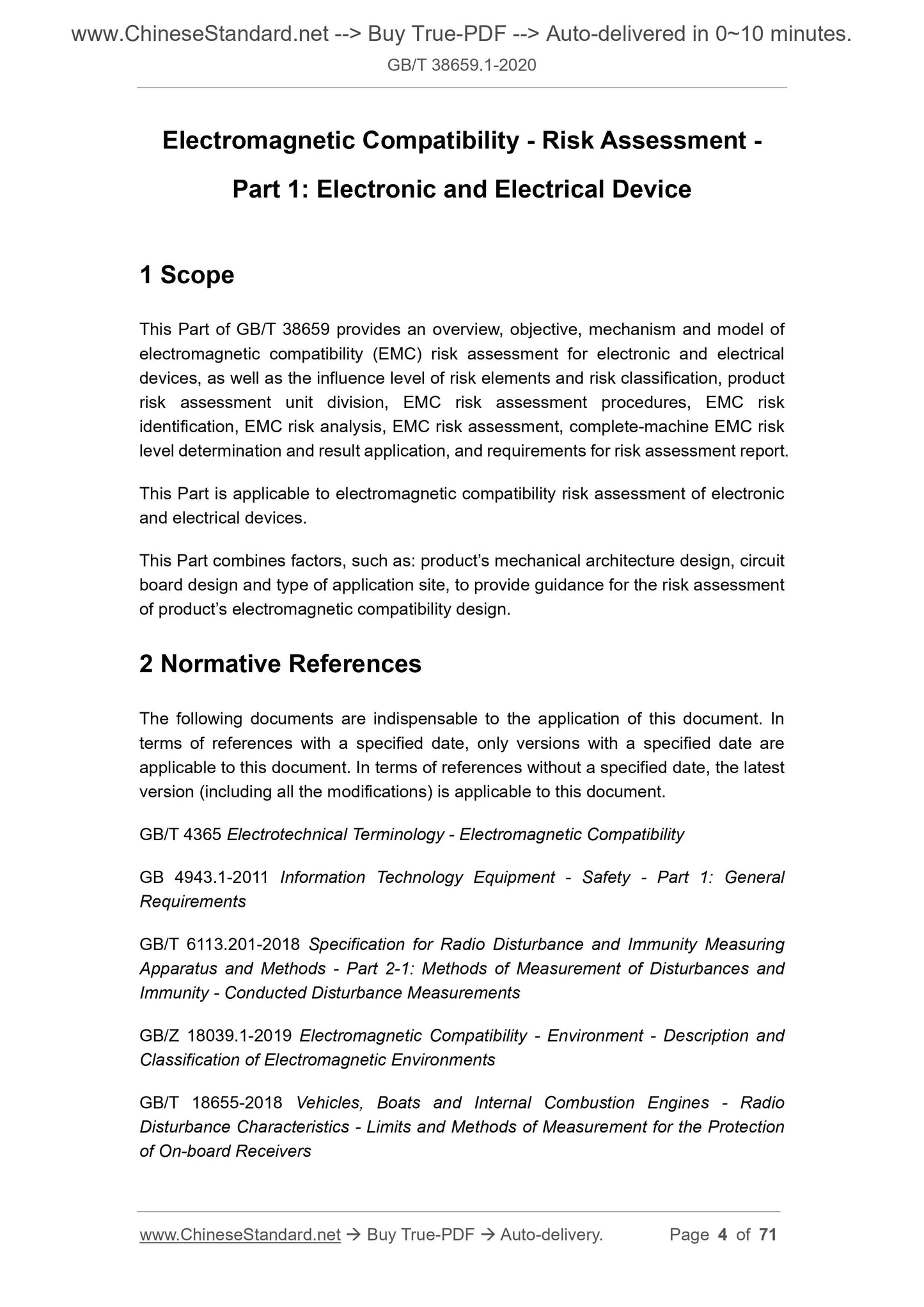
Scope
This Part of GB/T 38659 provides an overview, objective, mechanism and model of
electromagnetic compatibility (EMC) risk assessment for electronic and electrical
devices, as well as the influence level of risk elements and risk classification, product
risk assessment unit division, EMC risk assessment procedures, EMC risk
identification, EMC risk analysis, EMC risk assessment, complete-machine EMC risk
level determination and result application, and requirements for risk assessment report.
This Part is applicable to electromagnetic compatibility risk assessment of electronic
and electrical devices.
This Part combines factors, such as: product’s mechanical architecture design, circuit
board design and type of application site, to provide guidance for the risk assessment
of product’s electromagnetic compatibility design.
Basic Data
| Standard ID | GB/T 38659.1-2020 (GB/T38659.1-2020) |
| Description (Translated English) | Electromagnetic Compatibility - Risk Assessment - Part 1: Electronic and Electrical Device |
| Sector / Industry | National Standard (Recommended) |
| Classification of Chinese Standard | L06 |
| Classification of International Standard | 33.100 |
| Word Count Estimation | 46,497 |
| Date of Issue | 2020-03-31 |
| Date of Implementation | 2020-10-01 |
| Issuing agency(ies) | State Administration for Market Regulation, China National Standardization Administration |