Skip to product information
1 of 6

PayPal, credit cards. Download editable-PDF and invoice in 1 second!

GB/T 29055-2019 English PDF (GBT29055-2019)

GB/T 29055-2019 English PDF (GBT29055-2019)

Regular price $150.00 USD
Regular price Sale price $150.00 USD
Sale Sold out
Shipping calculated at checkout.
Delivery: 3 seconds. Download true-PDF + Invoice.
Get QUOTATION in 1-minute: Click GB/T 29055-2019
Historical versions: GB/T 29055-2019
Preview True-PDF (Reload/Scroll if blank)

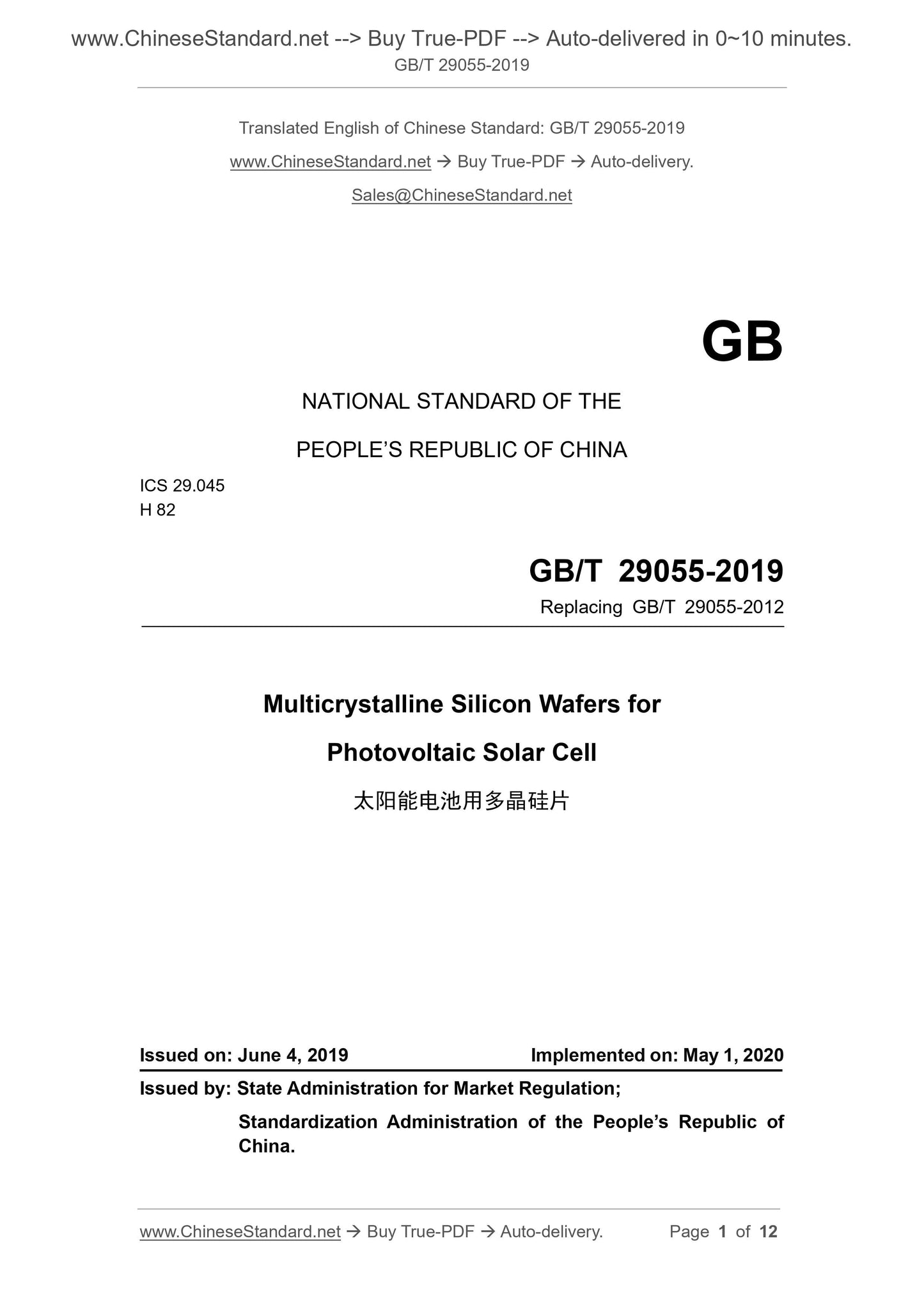
GB/T 29055-2019: Multi-crystalline silicon wafers for photovoltaic solar cell
GB/T 29055-2019
NATIONAL STANDARD OF THE
PEOPLE’S REPUBLIC OF CHINA
ICS 29.045
H 82
Replacing GB/T 29055-2012
Multicrystalline Silicon Wafers for
Photovoltaic Solar Cell
ISSUED ON: JUNE 4, 2019
IMPLEMENTED ON: MAY 1, 2020
Issued by: State Administration for Market Regulation;
Standardization Administration of the People’s Republic of
China.
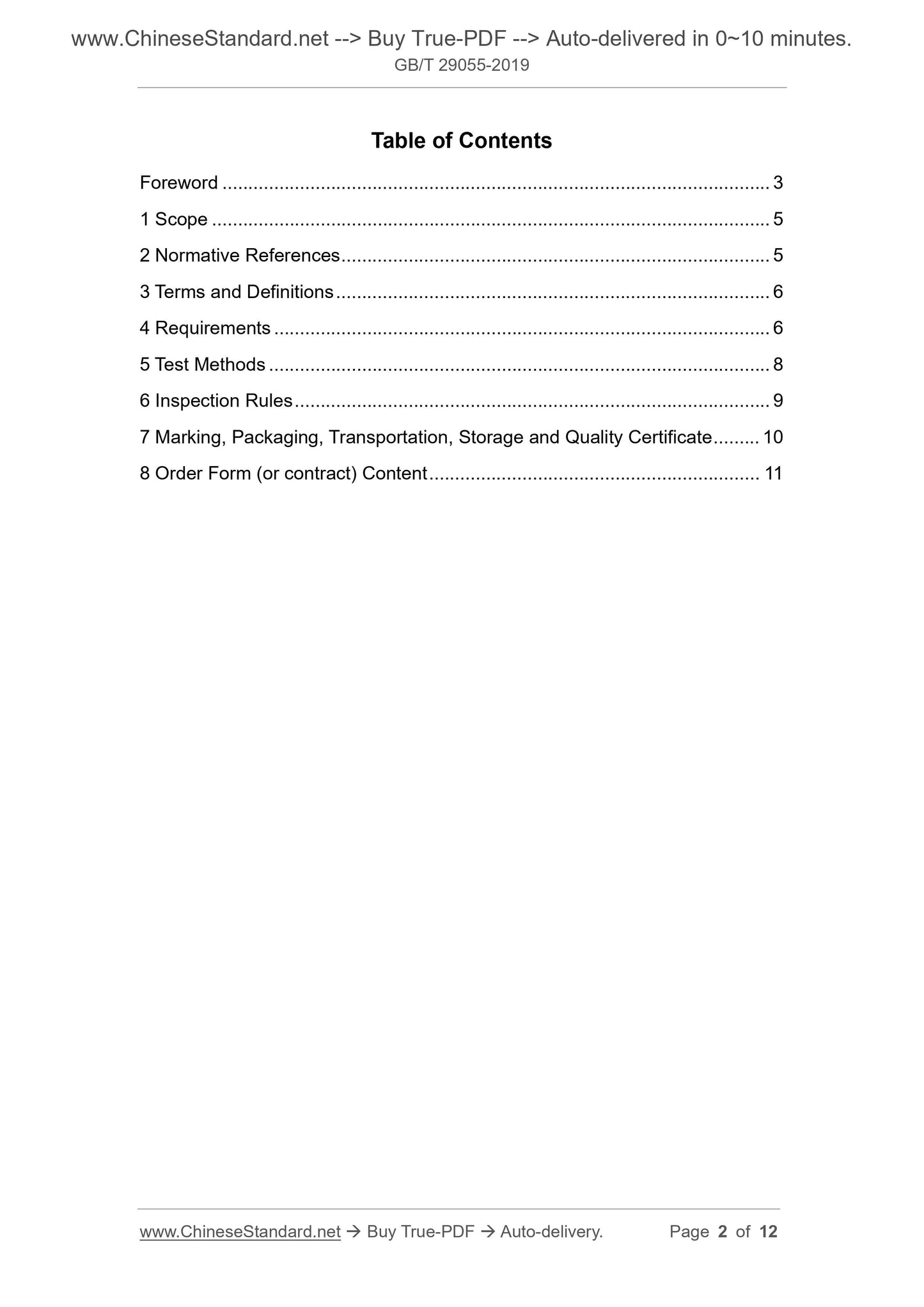
Table of Contents
Foreword ... 3 
1 Scope ... 5 
2 Normative References ... 5 
3 Terms and Definitions ... 6 
4 Requirements ... 6 
5 Test Methods ... 8 
6 Inspection Rules ... 9 
7 Marking, Packaging, Transportation, Storage and Quality Certificate ... 10 
8 Order Form (or contract) Content ... 11 
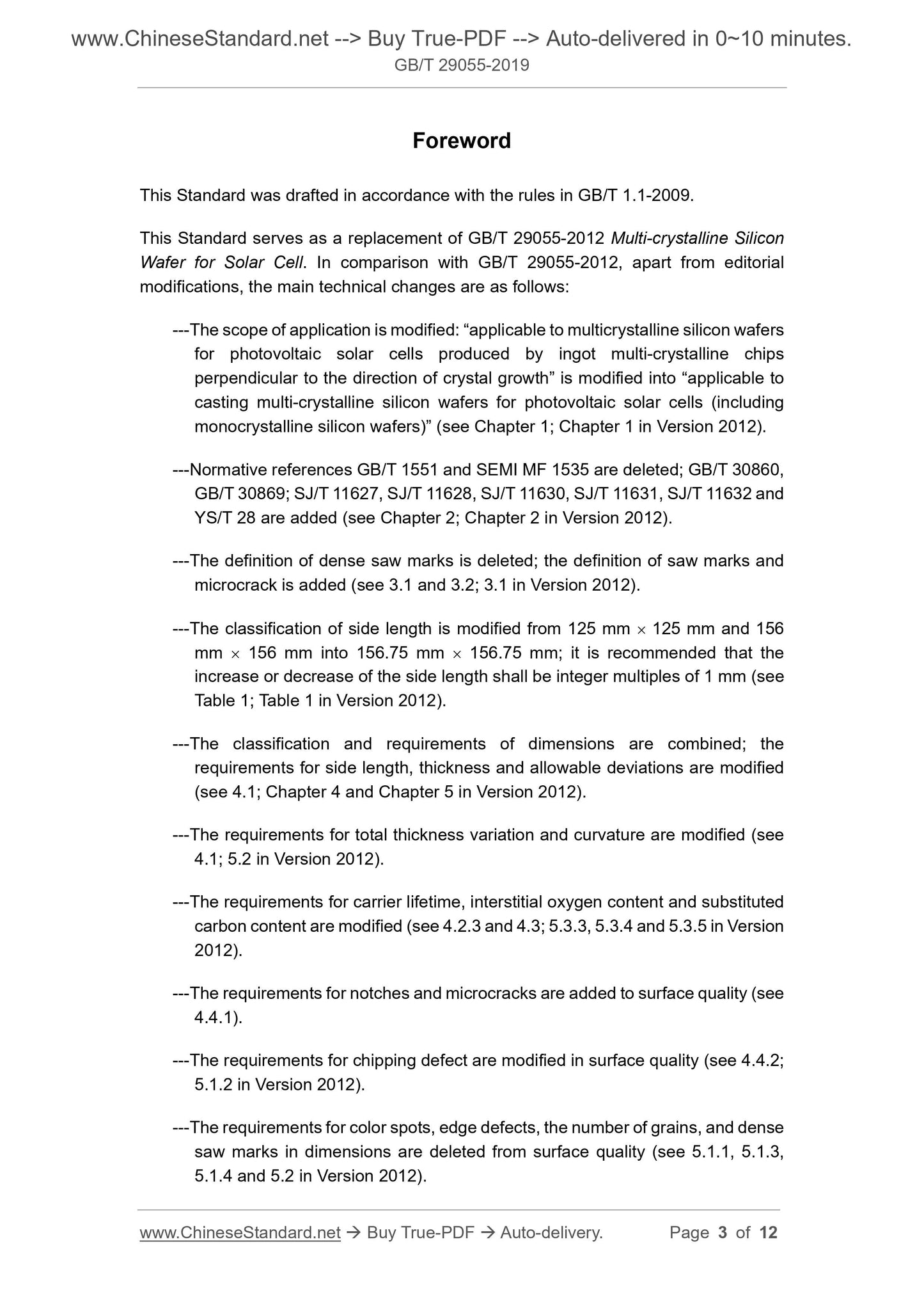
Foreword
This Standard was drafted in accordance with the rules in GB/T 1.1-2009.
This Standard serves as a replacement of GB/T 29055-2012 Multi-crystalline Silicon
Wafer for Solar Cell. In comparison with GB/T 29055-2012, apart from editorial
modifications, the main technical changes are as follows:
---The scope of application is modified: “applicable to multicrystalline silicon wafers
for photovoltaic solar cells produced by ingot multi-crystalline chips
perpendicular to the direction of crystal growth” is modified into “applicable to
casting multi-crystalline silicon wafers for photovoltaic solar cells (including
monocrystalline silicon wafers)” (see Chapter 1; Chapter 1 in Version 2012).
---Normative references GB/T 1551 and SEMI MF 1535 are deleted; GB/T 30860,
GB/T 30869; SJ/T 11627, SJ/T 11628, SJ/T 11630, SJ/T 11631, SJ/T 11632 and
YS/T 28 are added (see Chapter 2; Chapter 2 in Version 2012).
---The definition of dense saw marks is deleted; the definition of saw marks and
microcrack is added (see 3.1 and 3.2; 3.1 in Version 2012).
---The classification of side length is modified from 125 mm  125 mm and 156
mm  156 mm into 156.75 mm  156.75 mm; it is recommended that the
increase or decrease of the side length shall be integer multiples of 1 mm (see
Table 1; Table 1 in Version 2012).
---The classification and requirements of dimensions are combined; the
requirements for side length, thickness and allowable deviations are modified
(see 4.1; Chapter 4 and Chapter 5 in Version 2012).
---The requirements for total thickness variation and curvature are modified (see
4.1; 5.2 in Version 2012).
---The requirements for carrier lifetime, interstitial oxygen content and substituted
carbon content are modified (see 4.2.3 and 4.3; 5.3.3, 5.3.4 and 5.3.5 in Version
2012).
---The requirements for notches and microcracks are added to surface quality (see
4.4.1).
---The requirements for chipping defect are modified in surface quality (see 4.4.2;
5.1.2 in Version 2012).
---The requirements for color spots, edge defects, the number of grains, and dense
saw marks in dimensions are deleted from surface quality (see 5.1.1, 5.1.3,
5.1.4 and 5.2 in Version 2012).
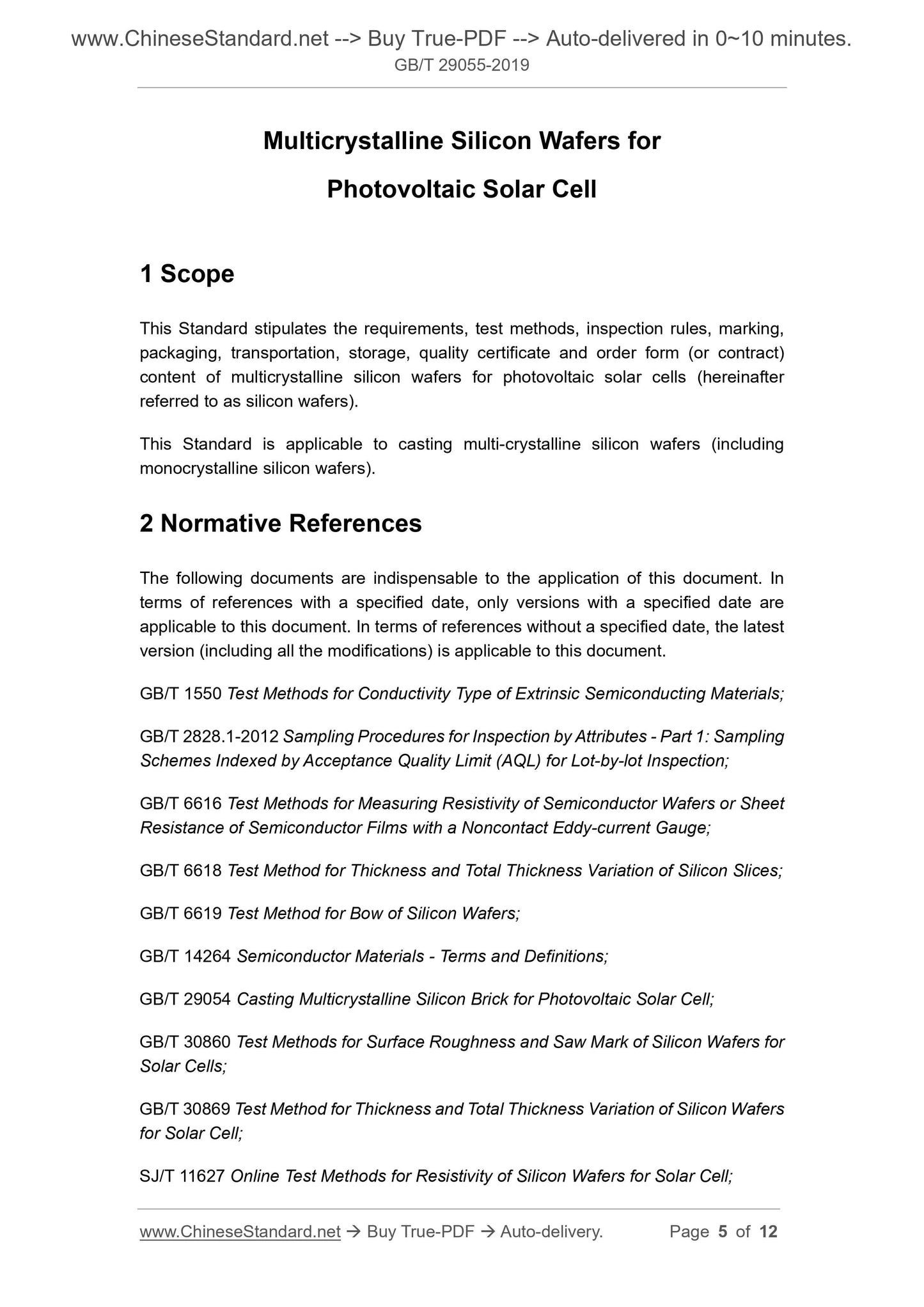
Multicrystalline Silicon Wafers for
Photovoltaic Solar Cell
1 Scope
This Standard stipulates the requirements, test methods, inspection rules, marking,
packaging, transportation, storage, quality certificate and order form (or contract)
content of multicrystalline silicon wafers for photovoltaic solar cells (hereinafter
referred to as silicon wafers).
This Standard is applicable to casting multi-crystalline silicon wafers (including
monocrystalline silicon wafers).
2 Normative References
The following documents are indispensable to the application of this document. In
terms of references with a specified date, only versions with a specified date are
applicable to this document. In terms of references without a specified date, the latest
version (including all the modifications) is applicable to this document.
GB/T 1550 Test Methods for Conductivity Type of Extrinsic Semiconducting Materials;
GB/T 2828.1-2012 Sampling Procedures for Inspection by Attributes - Part 1: Sampling
Schemes Indexed by Acceptance Quality Limit (AQL) for Lot-by-lot Inspection;
GB/T 6616 Test Methods for Measuring Resistivity of Semiconductor Wafers or Sheet
Resistance of Semiconductor Films with a Noncontact Eddy-current Gauge;
GB/T 6618 Test Method for Thickness and Total Thickness Variation of Silicon Slices;
GB/T 6619 Test Method for Bow of Silicon Wafers;
GB/T 14264 Semiconductor Materials - Terms and Definitions;
GB/T 29054 Casting Multicrystalline Silicon Brick for Photovoltaic Solar Cell;
GB/T 30860 Test Methods for Surface Roughness and Saw Mark of Silicon Wafers for
Solar Cells;
GB/T 30869 Test Method for Thickness and Total Thickness Variation of Silicon Wafers
for Solar Cell;
SJ/T 11627 Online Test Methods for Resistivity of Silicon Wafers for Solar Cell;
6616.
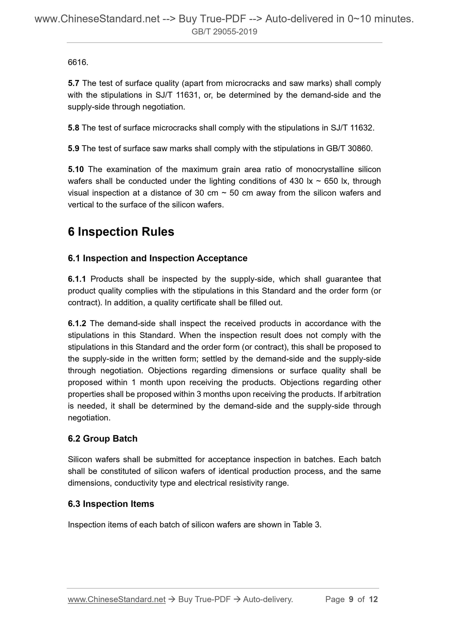
5.7 The test of surface quality (apart from microcracks and saw marks) shall comply
with the stipulations in SJ/T 11631, or, be determined by the demand-side and the
supply-side through negotiation.
5.8 The test of surface microcracks shall comply with the stipulations in SJ/T 11632.
5.9 The test of surface saw marks shall comply with the stipulations in GB/T 30860.
5.10 The examination of the maximum grain area ratio of monocrystalline silicon
wafers shall be conducted under the lighting conditions of 430 lx ~ 650 lx, through
visual inspection at a distance of 30 cm ~ 50 cm away from the silicon wafers and
vertical to the surface of the silicon wafers.
6 Inspection Rules
6.1 Inspection and Inspection Acceptance
6.1.1 Products shall be inspected by the supply-side, which shall guarantee that
product quality complies with the stipulations in this Standard and the order form (or
contract). In addition, a quality certificate shall be filled out.
6.1.2 The demand-side shall inspect the received products in accordance with the
stipulations in this Standard. When the inspection result does not comply with the
stipulations in this Standard and the order form (or contract), this shall be proposed to
the supply-side in the written form; settled by the demand-side and the supply-side
through negotiation. Objections regarding dimensions or surface quality shall be
proposed within 1 month upon receiving the products. Objections regarding other
properties shall be proposed within 3 months upon receiving the products. If arbitration
is needed, it shall be determined by the demand-side and the supply-side through
negotiation.
6.2 Group Batch
Silicon wafers shall be submitted for acceptance inspection in batches. Each batch
shall be constituted of silicon wafers of identical production process, and the same
dimensions, conductivity type and electrical resistivity range.
6.3 Inspection Items
Inspection items of each batch of silicon wafers are shown in Table 3.
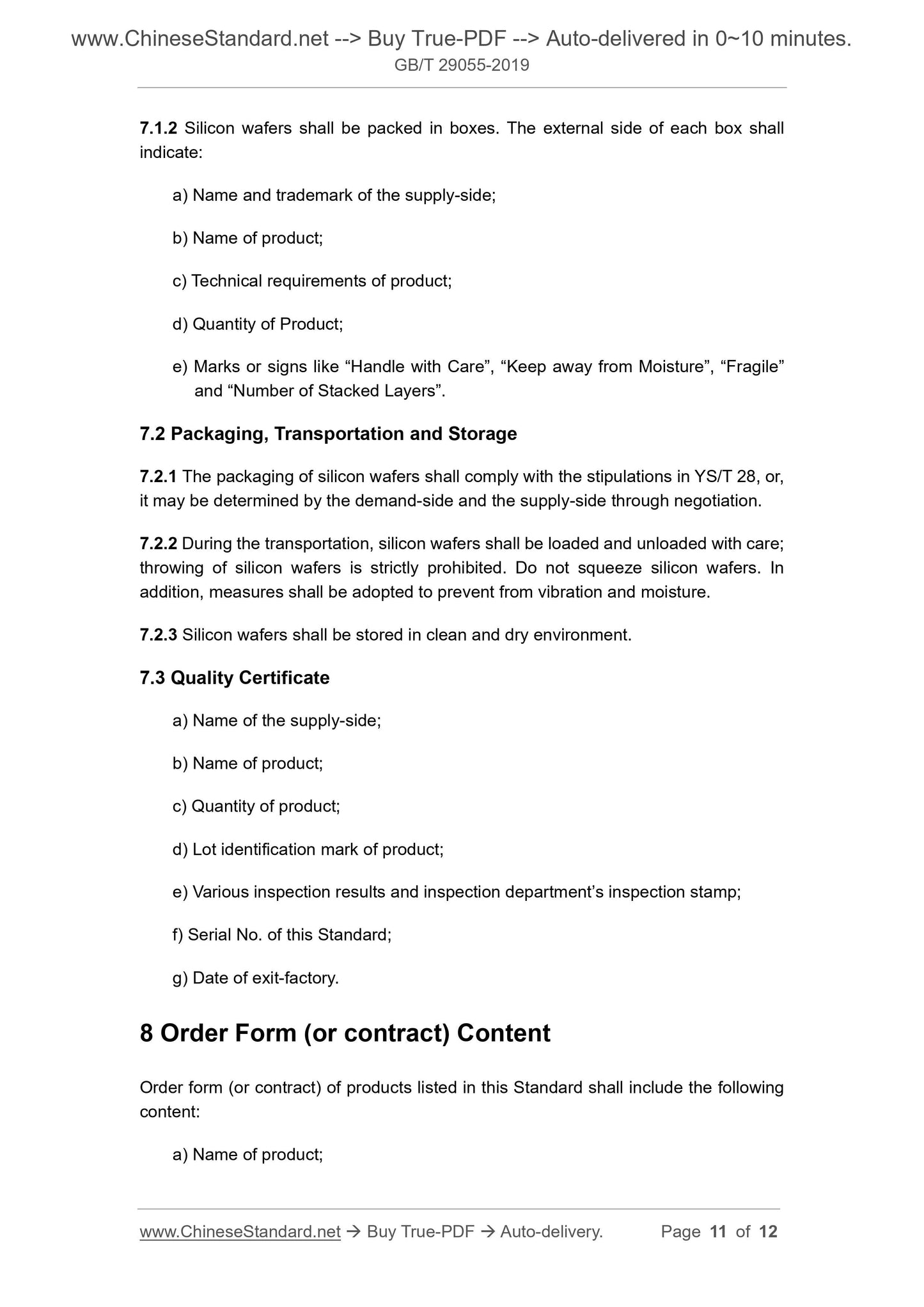
7.1.2 Silicon wafers shall be packed in boxes. The external side of each box shall
indicate:
a) Name and trademark of the supply-side;
b) Name of product;
c) Technical requirements of product;
d) Quantity of Product;
e) Marks or signs like “Handle with Care”, “Keep away from Moisture”, “Fragile”
and “Number of Stacked Layers”.
7.2 Packaging, Transportation and Storage
7.2.1 The packaging of silicon wafers shall comply with the stipulations in YS/T 28, or,
it may be determined by the demand-side and the supply-side through negotiation.
7.2.2 During the transportation, silicon wafers shall be loaded and unloaded with care;
throwing of silicon wafers is strictly prohibited. Do not squeeze silicon wafers. In
addition, measures shall be adopted to prevent from vibrat...
View full details