1
/
of
5
www.ChineseStandard.us -- Field Test Asia Pte. Ltd.
GB/T 16595-2019 English PDF (GB/T16595-2019)
GB/T 16595-2019 English PDF (GB/T16595-2019)
Regular price
$140.00
Regular price
Sale price
$140.00
Unit price
/
per
Shipping calculated at checkout.
Couldn't load pickup availability
GB/T 16595-2019: Specification for a Universal Wafer Grid
Delivery: 9 seconds. Download (and Email) true-PDF + Invoice.Get Quotation: Click GB/T 16595-2019 (Self-service in 1-minute)
Newer / historical versions: GB/T 16595-2019
Preview True-PDF
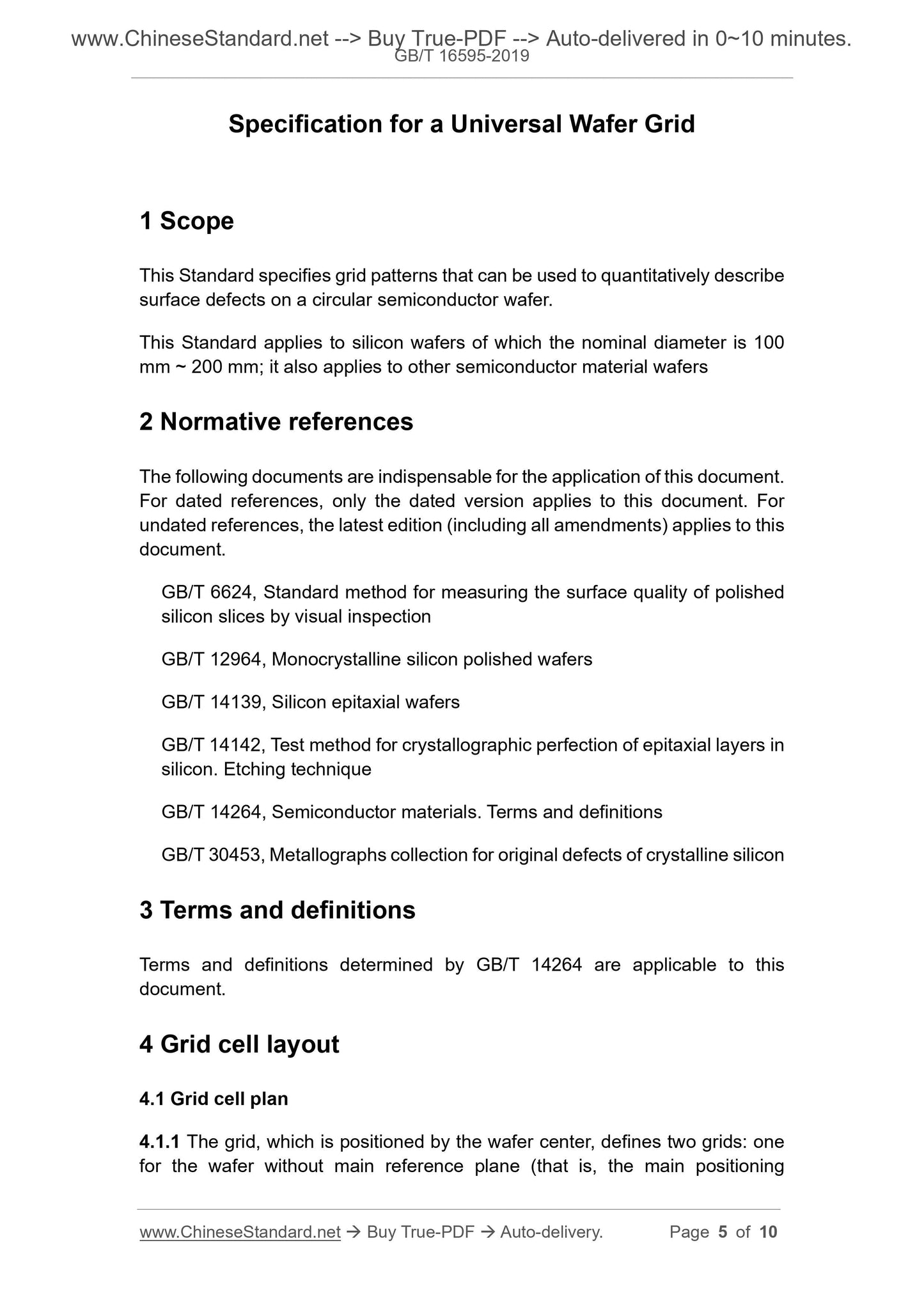
Scope
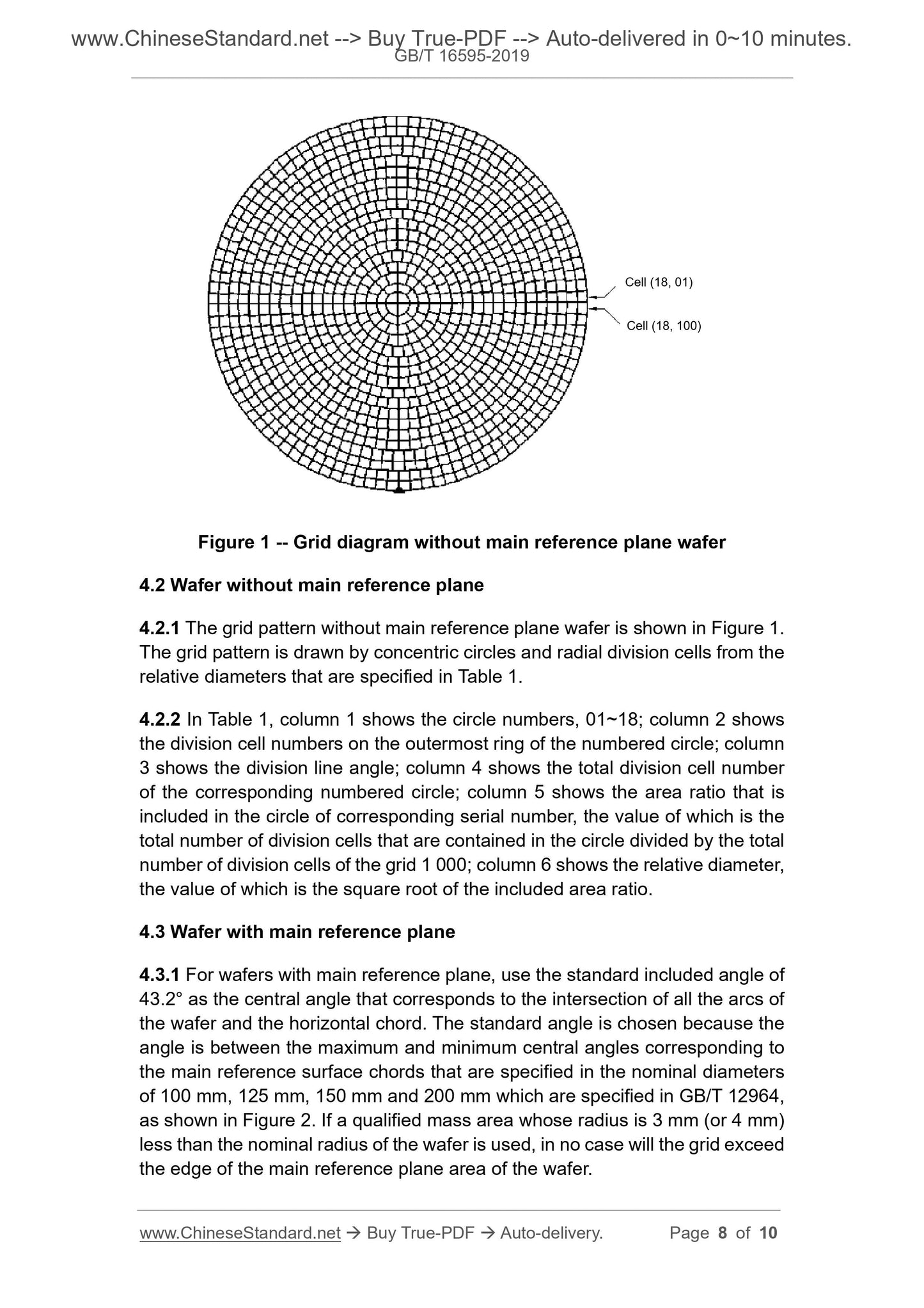
This Standard specifies grid patterns that can be used to quantitatively describesurface defects on a circular semiconductor wafer.
This Standard applies to silicon wafers of which the nominal diameter is 100
mm ~ 200 mm; it also applies to other semiconductor material wafers
Basic Data
| Standard ID | GB/T 16595-2019 (GB/T16595-2019) |
| Description (Translated English) | Specification for a Universal Wafer Grid |
| Sector / Industry | National Standard (Recommended) |
| Classification of Chinese Standard | H80 |
| Classification of International Standard | 29.045 |
| Word Count Estimation | 10,135 |
| Date of Issue | 2019-03-25 |
| Date of Implementation | 2020-02-01 |
| Issuing agency(ies) | State Administration for Market Regulation, China National Standardization Administration |
Share